Park Air Electronics Series 3000 Summing-Up ... with a Happy Ending
24 minute read
This post is part of the series 'Park Air Electronics Series 3000':
 The PAE 3000 Series is a range of Air-Band transceivers, transmitters and receivers, manufactured by Park Air Electronics in the 1990s :-
Transceivers: PAE 3010 - VHF. PAE 3030 - UHF. PAE 3050 - VHF/UHF.
Transmitters: PAE 3130 - UHF. PAE 3150 - VHF/UHF.
Receivers: PAE 3230 - UHF. PAE 3250 - VHF/UHF.
The equipment is modular and makes extensive use of BITE (Built In Test Equipment), which actually makes the type relatively easy to repair, until you realise that the Technical Handbook doesn't quite cover everything. Then there's the fact that the Mod-Strike label is struck off to number 5, but there is nothing in the manual to document these modifications. That said, I actually like these. In the last six months I have repaired no less than seven of them ... three 3010s and four 3030s. Although one of the 3030s is still awaiting a unique and difficult to obtain replacement part ... highlighting an issue not uncommon with 30 year-old equipment.
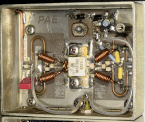
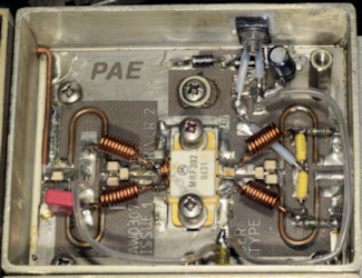
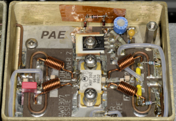
The Synthesiser is a tried and tested design typical of the day. The Power Amplifier modules are a thing of beauty and gloriously over-rated. By that, I mean that the PAs (VHF and UHF) are run so far below spec. that they will likely run full power all day, every day!
The Power Supply is nothing special and logically split into two parts. One part catering for the Power Amplifiers whilst the other provides for everything else.
Transmitted and Received audio is made available via a rear panel connector for connection to a recording or logging system ... very important when you consider the responsibility of the operators. All Series 3000 equipment can be controlled remotely and the receivers can also be fitted with a Guard Receiver; a single-frequency stand-alone receiver module tuned to an appropriate emergency frequency. The type is simple to operate, with all user-input via an easy to navigate Front Panel.
It is however very heavy, with each single-band transceiver weighing 32Kg. Because of its modular nature, two types of card extenders are required to gain access to various test-points etc. Although the sides of the unit fold down to give access to the Power Amps and the PA Power Regulators, over 65 screws first need to be removed!
Although the Power Supply is relatively uncomplicated, there are potential issues with it. On the Mains input side, the schematic diagram over-simplifies the voltage selector and primary windings. See my article on the 3030 in this series. Also, because of the limited space available, the wiring to the two voltage selector switches actually fits into the hole in the centre of the toroidal transformer. I know that the wiring is insulated, but placing metal into this void is a catastrophe waiting to happen should there be contact with the chassis. Since the two switches are not centred on the void, it is possible for one of the Mains Selector switches to make contact with the transformer and rupture the insulation.
The photograph on the left shows the main PSU board. The components in the top left of the photograph form a small Switched Mode regulator whose only purpose is to provide a negative supply from which the -10V rail is derived. There may be a bit of a design oversight here. By nature of the design, the three (in a row) electrolytic capacitors in this circuit are stressed much more than they would be if this were a linear regulator. This is because in this circuit, as with many switching regulators, the ripple current can be as high as 100KHz, and is the reason why high-quality, high-temperature electrolytics are the norm. However, in this circuit, the 'at risk' capacitors are standard low-frequency types which lack the capability to cope with high-frequency ripple currents. In which case, they heat up and deteriorate, capacitance drops and ESR rises. In most of the PAE transceivers that I have repaired, at least two of these capacitors have exhibited an ESR of over twenty! In three of them the Zener diode in series with the regulator has been open-circuit ... no doubt due to the capacitors failing. The worst case scenario is a failed -10V line, but often the fault manifests as a -10V line that takes a few seconds to reach potential, and the BITE picks up on this and flags an error. Thus, the best practice is to replace C7 and C9 with high quality types regardless because if they haven't failed yet, they will in due course.
Elsewhere, there appears to be an apparent preference for 78Sxx regulators. This is the 2A version of the ubiquitous 1A TO220 3-terminal regulator. I encountered a 78S10 on the Synthesiser module that had got so hot that it had literally caramelised the PCB. This was likely caused by a genuine fault elsewhere ... a blown PAL on the Remote Control Decoder Module, Module-5. The Synthesiser was rendered inoperative. Having removed the faulty Module-5, the Synthesiser worked and the 78S10 no longer gets hot. However, as with all regulators, the actual power dissipated is the product of the voltage between the input and output and the current drawn. Using a 2A regulator where a 1A one will suffice, will not incur less heat. It will still get very hot if you don't provide adequate heat-sinking.
Also on the Synthesiser module ... there is a little TO-92 LM317LZ. Clearly this gets hot. I know, because the white plastic-spacer-thing between it and the board has turned to 'chalk' in all cases. Touch it and it disintegrates ... the spacer, not the regulator ... another design oversight, methinks.
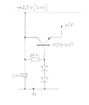
As can be seen in the photograph above, PAE also modified the bias circuit to allow more precise setting of the Quiescent Current and perhaps as a consequence, keep the temperature of the MJE340 down. Originally two 1N4001s in series provided around 1.3V on the Base of the transistor. These have been replaced with three 1N4148s (I think) in parallel with a 1K potentiometer. Note the Kapton tape on the side wall where the diodes are glued in place.
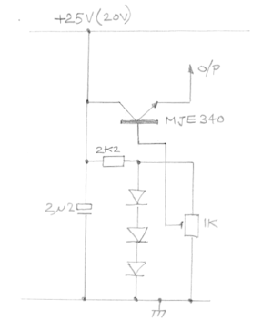
The voltage on the Collector of the MJE340 is +25V on AM and reduced to +20V on FM. Interestingly, the schematic in the Technical Manual shows that this stage and the Pre-Driver stage were both originally supplied from a +15V line. This is very likely why it was originally thought unnecessary to provide a heatsink for the MJE340.
As far as the Technical Manual for the PAE Series 3000 is concerned, I could write a book detailing it's failings. But that would be unfair. In some respects, it reminds me of the Technical manual for the Racal MA79, which itself is a very difficult document to come by, unless you want a photocopy of a very bad photocopy. I am told that Racal considered the MA79 to be too complex to expect the End User to carry out their own repairs. Consequently, what passes for a Technical Manual reads like reworked engineers notes in places.
The Technical Manual for the PAE Series 3000 equipment reads like it was written by design engineers for those who had an intimate knowledge of it. This wasn't too much of a problem for me since I have been working with RF products for the last fifty years. And since the Series 3000 was designed thirty years ago, the technology is relatively straight-forward. That isn't to say that the learning curve was not steep.
The first thing that I noticed was the complete lack of amendments. There are pages at the front for listing such things but there are no entries. This, despite the fact that the MOD-Strike Label on the rear of each transceiver was struck off to 5 ... implies at least five modifications or changes to the hardware. Park Air were contacted for a list of modifications, but my client was politely informed that such information was 'not the sort of information that would be passed on to the end-user'. They, Park Air were also apparently surprised that someone wished to repair thirty year-old equipment.
Issues with the manual can be divided into several categories ... Spelling mistakes or mis-descriptions, errors in circuit diagrams, and things which are simply not there! Having spent thirteen years at Racal, at a site where Quality Control was paramount, it isn't difficult to notice where something has gone to print without proper proof-reading. There are at least three things in the technical manual which made me laugh. One is the use of BRAKE in the Items List with respect to Momentary-Break switches. This spelling error occurs dozens of times. Then there are a couple of 'funnies' which are clearly the result of someone's (badly) hand-written notes being transcribed incorrectly. The first one is on the circuit diagram for the Synthesiser, where the 27256 EPROM is identified as 12127128 ... woops!, and the second is in the Items List for the BITE Assembly board where the 8031 Micro-Controller is listed as an MRO-Controller.
All these errors are minor compared to what I found in the technical description of the Remote-Control Decoder Module. There are some major documentation issues relating to other modules, but these have already been discussed in previous articles in this series. Without the 'other end' of the link at hand, this is the ONLY module within the transceiver that I have not been able to test fully, apart from using the BITE. Up until now I had successfully repaired six such transceivers, with four of these already back in the rack and 'on-air' tested via the remote link. The fifth one, a 3010 was repaired and prepared for transit whilst I tackled the final two, both 3030s and both apparently showing the same fault: the frequency display showing all zeros. One of these was little more than a faulty PSU board. But the final 3030 was destined to cause much frustration and gnashing of teeth.
 BITE was suggesting that there was something wrong with the Synthesiser, but a simple substitution proved this not to be the case. Although the BITE will report faults relating to the Remote-Control Decoder (Module-5), any reported codes are meaningless since nowhere in the manual is there a list of 'Module-5' failure codes. With that in mind, I simply 'pulled' module-5 and switched on the transceiver. Imagine my surprise when the 3030 burst into life. I then initiated BITE and it reported a PASS!
See the photograph on the right. Notice the dark spot in the middle of the label on the chip next to the 8031 Micro-controller. Initially this looked like a greasy spot, but it turned out to be a 'burn'. The adhesive had been so cooked that the label was effectively bonded to the chip at that point.
Replacing damaged EPROMs is relatively straight-forward, provided you have access to the firmware and a suitable programmer. Recently these have been relatively inexpensive to come by, and the XGecu TL866 is definitely worth the investment. However, the damaged IC on the Remote-Control Decoder turned out to be a PAL ... a different 'animal' altogether.
 PAL stands for Programmable Array Logic; making it possible to replace multiple SSI/MSI ICs with a single programmable array and thus reducing the chip count. I first came across these whilst working at Racal Defence about 40 years ago.
The 22V10 has an impressive 132 x 44 programable AND array and no less than ten programable Macrocells. These devices cannot be readily 'read' since they do not conform to the data structure found in EPROMs etc. But as long as you have the 'map' that was used to configure the array, it is easy to configure a replacement chip using readily available hardware and software. But here's where 'we' ran up against a problem. Despite appealing to the good people at Park Air, as was the case in the past, they informed 'us' that information on the PALs (there are two) in the Remote-Control Decoder could not be provided.
Not only that, we were told that all support for the Series 3000 ceased as far back as 1998 or thereabouts, and that the information that we sought no longer existed. Did that imply that it had been thrown out, or were they (Park Air) simply totally disinterested in providing support? Granted, the type is around thirty years old, but by my reckoning and from what they say, it sounds like they stopped supporting it less than ten years after it went into production! This revelation had both myself and my client completely 'stunned' since both of us had previously worked for major UK Defence Electronics companies that regularly provided very long-term customer support. Not only had Park Air made it clear that support for the type had not been readily available since 1998, they had also declined to provide any information relating to the five mod-strikes, and had also informed my client that such information was never made available to the end-user! Was this actually company policy?
Anyway, back to the current problem ... the faulty PAL. I found that the transceiver would function perfectly as a stand-alone unit without Module-5 fitted. The BITE clearly detected its lack of presence and did not report any issues. However, if Module-5 was installed and IC11 was missing (or faulty), BITE flagged a fault. Whereas a 'locally' operated transceiver is perfectly feasible in a civil ATC context, it is most definitely NOT an option when it is part of a tactical radar installation like the BAe Systems AR-327 (aka T101a). I obtained a couple of 'blank' 22V10s and sent these, along with a working PAL down to my client. As suspected, the security fuse in the working PAL had been blown to prevent readback of the internal programmed pattern. It is probably worth noting here that although AMD CE22V10s have this security fuse, it would appear that Cypress 22V10s might not have this feature.
Being an RF man, logic and such things is not my strong suit. My client informed me that if the PAL was 'protected', they might have to painstakingly etch away the top of the IC in order to wedge-bond a replacement fuse-link in place. But first, his resident expert in such things had a plan whereby patterns would be 'thrown' at a PAL to see if they could mimic the programmed pattern. But that relied on understanding what the PAL was supposed to do, and Park Air had already demonstrated that they weren't interested in helping.
Right: IC11 on the Remote-Control Decoder appears to be primarily associated with rear-panel PTT control, coming onto the board via CN1 pin 20A. From what I can see, there are six (or 7?) inputs and three outputs. Pin 2 is a Mute signal from the Guard Receiver (if fitted). Pin 5 is 'PTT Remote', generated locally (on-board) by TR1. Pin 6 (and perhaps at one time pin 7) handles the Hardwire PTT from the Facilities 2 connector on the rear panel. Pins 1, 3 and 4 are signals from the Microcontroller (IC1)
The three outputs from the PAL are ... Pin 22 which goes to IC1, Pin 21 which goes to the TX Control Module as PTT, and pin 23 provides PTT Select which is an internal control line for enabling Multiplexers IC32 and IC27.
Within the dotted area marked 'Optional' R36 should be R122. As you can see there is already scope for confusion with two different control signals with very similar names ... 'PTT Remote' which is generated on-board and 'Hardwire PTT' which comes from a connector on the rear panel, and thus can be considered Remote PTT. Well done Park Air! And the confusion doesn't end there ...
Para 22 in the Remote-Control Decoder circuit description is, to put it mildly, rubbish. It is entitled Hardwire PTT and reads thus ...
An external hardwire PTT can be configured through the facilities 2 connector and can be set to respond to a ground, or a high (nominally 6V dc) signal (refer to para 10). The signal is connected to the CPU through IC13e and IC11.
Yes, the signal known as Hardwire PTT does come from the Facilities 2 connector, BUT because of D21 (1N4148), this can be nothing other than a ground connection, i.e. only an Active-Low signal will work. This signal does NOT go to the CPU (mis-named Microcontroller IC1) via IC11 and IC13. Pin 23 of IC11 is an output, NOT and input ... and IC13 is a Hex Open-Drain N-channel Buffer and pin 13 (output) is connected to the Enable pins on multiplexers IC32 and IC27. The only output (presumably PTT-related) from IC11 that goes to IC1, comes from pin 22.
As noted above, Para 22 refers the reader to Para 10. This describes the function of links 2 and 3 on the Remote-Control Decoder. Here, the Active-High signal is given as nominally +24V! Whether it is +6V or +24V, neither will work due to the presence of D21. Note too that Link 2 actually has nothing to do with the Hardwire PTT signal from the facilities connector; rather, it is associated with the 2930Hz PTT-tone via Transformer T4 ... see left.
So ... where's the happy ending?
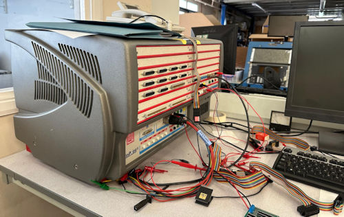
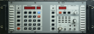
One of my client's engineers, who has a background in chip design, and is apparently very good at it, suggested that it might be possible to ascertain the 'contents' of the PAL (IC11) by 'throwing' patterns at a PAL until it 'mimicked' a known good one. Much easier than slicing away the top and examining the contents under a microscope. After all, the chip only has seven inputs and three outputs. So with the machine on the right, a logic analyser and a 4-channel 'scope, he spent several weeks 'throwing' patterns at a PAL and eventually came up with something that he was 99% sure was a match.
The 'new' PAL, along with an original working one were subsequently sent up to me for testing. It worked! Since IC11's only purpose is to cater for External or Remote PTT, I was very quickly able to verify that the new PAL was working correctly.
Initially I couldn't get either PAL to do anything ... and then it struck me. I had spent the last six months working on these transceivers with them in LOCAL mode. Although the manual clearly states that PTT can be initiated via the 'Facilities 2' connector on the rear panel, what it doesn't say (and I have checked) is that for the connectors on the rear panel to work, the transceiver MUST be set to REMOTE mode.
Not only that. With the manual talking about ac (tone) and dc operation, there was always a question about link settings on the Remote Control Decoder board. Was a simple PTT connection considered as dc? And if tone-PTT (2930Hz tone superimposed on the TX audio) was applied, was that instead of Hardwire-PTT? At the end of the day, with the board configuration un-touched (as received), and the transceiver in REMOTE mode, I found that with 0dbm of 2930Hz applied via the 9-way D-type Remote-1 connector, the transceiver automatically went to Transmit. And with the tone removed, it dropped back to Receive. With no tone present, I found that initiating Hardwire-PTT via the Facilities-2 connector also initiated Transmit.
And there we have our happy ending! Seven faulty Park Air transceivers repaired. I've said it before, and I'll say it again ... I actually like these!
Some light reading ... PAE 3000 manuals:
Operator's Manual
Technical Handbook ... as said, this document contains many errors.
- Park Air Electronics 3030
- Park Air Electronics 3010
- Park Air Electronics Series 3000 Summing-Up ... with a Happy Ending
June 2026
PAE 3030
Transceivers: PAE 3010 - VHF. PAE 3030 - UHF. PAE 3050 - VHF/UHF.
Transmitters: PAE 3130 - UHF. PAE 3150 - VHF/UHF.
Receivers: PAE 3230 - UHF. PAE 3250 - VHF/UHF.
The equipment is modular and makes extensive use of BITE (Built In Test Equipment), which actually makes the type relatively easy to repair, until you realise that the Technical Handbook doesn't quite cover everything. Then there's the fact that the Mod-Strike label is struck off to number 5, but there is nothing in the manual to document these modifications. That said, I actually like these. In the last six months I have repaired no less than seven of them ... three 3010s and four 3030s. Although one of the 3030s is still awaiting a unique and difficult to obtain replacement part ... highlighting an issue not uncommon with 30 year-old equipment.
Pros & Cons:
Aside from it's use of no less than three 8031 Microcontrollers, the RF side is very straightforward. As with Racal's 1792 and 3700 series, the receiver is basically a series of broadband gain blocks and mixers, with selectivity provided by filters. The receiver is split over two modules, which oddly, are not side-by-side.The Synthesiser is a tried and tested design typical of the day. The Power Amplifier modules are a thing of beauty and gloriously over-rated. By that, I mean that the PAs (VHF and UHF) are run so far below spec. that they will likely run full power all day, every day!
The Power Supply is nothing special and logically split into two parts. One part catering for the Power Amplifiers whilst the other provides for everything else.
Transmitted and Received audio is made available via a rear panel connector for connection to a recording or logging system ... very important when you consider the responsibility of the operators. All Series 3000 equipment can be controlled remotely and the receivers can also be fitted with a Guard Receiver; a single-frequency stand-alone receiver module tuned to an appropriate emergency frequency. The type is simple to operate, with all user-input via an easy to navigate Front Panel.
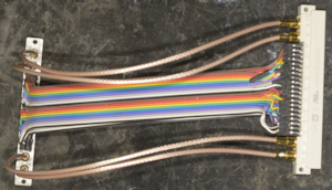
Home-made CN1 Extender.
It is however very heavy, with each single-band transceiver weighing 32Kg. Because of its modular nature, two types of card extenders are required to gain access to various test-points etc. Although the sides of the unit fold down to give access to the Power Amps and the PA Power Regulators, over 65 screws first need to be removed!
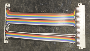
Home-made CN2 Extender.
Although the Power Supply is relatively uncomplicated, there are potential issues with it. On the Mains input side, the schematic diagram over-simplifies the voltage selector and primary windings. See my article on the 3030 in this series. Also, because of the limited space available, the wiring to the two voltage selector switches actually fits into the hole in the centre of the toroidal transformer. I know that the wiring is insulated, but placing metal into this void is a catastrophe waiting to happen should there be contact with the chassis. Since the two switches are not centred on the void, it is possible for one of the Mains Selector switches to make contact with the transformer and rupture the insulation.
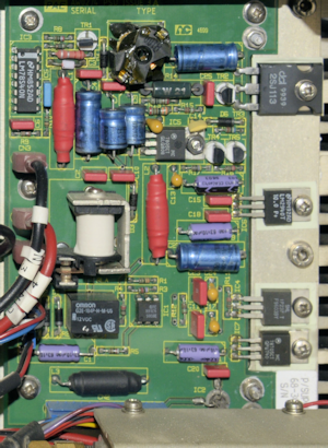
Main PSU Board
The photograph on the left shows the main PSU board. The components in the top left of the photograph form a small Switched Mode regulator whose only purpose is to provide a negative supply from which the -10V rail is derived. There may be a bit of a design oversight here. By nature of the design, the three (in a row) electrolytic capacitors in this circuit are stressed much more than they would be if this were a linear regulator. This is because in this circuit, as with many switching regulators, the ripple current can be as high as 100KHz, and is the reason why high-quality, high-temperature electrolytics are the norm. However, in this circuit, the 'at risk' capacitors are standard low-frequency types which lack the capability to cope with high-frequency ripple currents. In which case, they heat up and deteriorate, capacitance drops and ESR rises. In most of the PAE transceivers that I have repaired, at least two of these capacitors have exhibited an ESR of over twenty! In three of them the Zener diode in series with the regulator has been open-circuit ... no doubt due to the capacitors failing. The worst case scenario is a failed -10V line, but often the fault manifests as a -10V line that takes a few seconds to reach potential, and the BITE picks up on this and flags an error. Thus, the best practice is to replace C7 and C9 with high quality types regardless because if they haven't failed yet, they will in due course.
Elsewhere, there appears to be an apparent preference for 78Sxx regulators. This is the 2A version of the ubiquitous 1A TO220 3-terminal regulator. I encountered a 78S10 on the Synthesiser module that had got so hot that it had literally caramelised the PCB. This was likely caused by a genuine fault elsewhere ... a blown PAL on the Remote Control Decoder Module, Module-5. The Synthesiser was rendered inoperative. Having removed the faulty Module-5, the Synthesiser worked and the 78S10 no longer gets hot. However, as with all regulators, the actual power dissipated is the product of the voltage between the input and output and the current drawn. Using a 2A regulator where a 1A one will suffice, will not incur less heat. It will still get very hot if you don't provide adequate heat-sinking.
Also on the Synthesiser module ... there is a little TO-92 LM317LZ. Clearly this gets hot. I know, because the white plastic-spacer-thing between it and the board has turned to 'chalk' in all cases. Touch it and it disintegrates ... the spacer, not the regulator ... another design oversight, methinks.
RFPA Design issue:
As previously discussed in my article on the PAE 3030, there is an potential issue with the bias supply transistor (MJE340) in the second driver stage over-heating, with a temperature of +65C being recorded. My client had managed to 'lay his hands' on a couple of salvaged UHF RFPAs. These were sent on to me as potential spares. Judging by the date-codes on some of the RF devices, these were manufactured some time in 1997 .... late in the production life of the type. On examining these, it was immediately clear that PAE had eventually realised that there was a problem with the pass-transistor in the bias supply in the second driver stage. To that extent, where the MJE340 had originally been isolated from the main heat-sink, it was now to some degree, in thermal contact with the box, and thus with the heatsink with the addition of a copper plate. Without stripping it down, I cannot comment on the integrity of this 'fix'. However tests showed that the maximum temperature achieved on the MJE340 was now +35C ... a vast improvement on +65C! In contrast, my solution to the problem, which involves mounting the transistor on the side-wall of the compartment results in a maximum MJE340 temperature of +30C.
Severely burned Duroid.
My solution to the problem.
PAE's solution.
Original bias circuit.
As can be seen in the photograph above, PAE also modified the bias circuit to allow more precise setting of the Quiescent Current and perhaps as a consequence, keep the temperature of the MJE340 down. Originally two 1N4001s in series provided around 1.3V on the Base of the transistor. These have been replaced with three 1N4148s (I think) in parallel with a 1K potentiometer. Note the Kapton tape on the side wall where the diodes are glued in place.
Revised bias circuit.
The voltage on the Collector of the MJE340 is +25V on AM and reduced to +20V on FM. Interestingly, the schematic in the Technical Manual shows that this stage and the Pre-Driver stage were both originally supplied from a +15V line. This is very likely why it was originally thought unnecessary to provide a heatsink for the MJE340.
Technical Manual:
When I worked at Racal (1979 - 1992), my job latterly entailed working with the design engineers to ensure that what they designed was testable, and then designing any 'Special Test Equipment' as required. As a result, I wrote a lot of test procedures. At Racal, we had strict procedures governing how these procedures were written. For want of a better description, it was a two stage process that resulted in not one but two documents. The initial document outlined WHAT was to be tested, not how. The second document detailed HOW the testing was to be carried out and listed what test equipment was required. This document had to be written such that ANYONE could carry out the test. This was very important since my place of work was more of a design facility and product manufacture was likely to be transferred elsewhere. Also, if the End-User was expected to carry out their own repairs, as was often the case, it was vitally important that test procedures were clear and concise and did not require an intimate knowledge of the board or module.As far as the Technical Manual for the PAE Series 3000 is concerned, I could write a book detailing it's failings. But that would be unfair. In some respects, it reminds me of the Technical manual for the Racal MA79, which itself is a very difficult document to come by, unless you want a photocopy of a very bad photocopy. I am told that Racal considered the MA79 to be too complex to expect the End User to carry out their own repairs. Consequently, what passes for a Technical Manual reads like reworked engineers notes in places.
The Technical Manual for the PAE Series 3000 equipment reads like it was written by design engineers for those who had an intimate knowledge of it. This wasn't too much of a problem for me since I have been working with RF products for the last fifty years. And since the Series 3000 was designed thirty years ago, the technology is relatively straight-forward. That isn't to say that the learning curve was not steep.
The first thing that I noticed was the complete lack of amendments. There are pages at the front for listing such things but there are no entries. This, despite the fact that the MOD-Strike Label on the rear of each transceiver was struck off to 5 ... implies at least five modifications or changes to the hardware. Park Air were contacted for a list of modifications, but my client was politely informed that such information was 'not the sort of information that would be passed on to the end-user'. They, Park Air were also apparently surprised that someone wished to repair thirty year-old equipment.
Actually, there is a very reasonable reason why someone in the UK, seeking to repair such equipment might be considered odd, or even questionable. Being professional Air-Band transceivers from the 1990s, they only cater for 25KHz channel-spacing. As far back as 2005 it was obvious that the 25KHz system was not going to be able to safely accommodate the ever increasing needs of air-traffic-control in Europe and North America. Thus a new system based on 8.33KHz spacing was envisaged and implemented. Although that implies frequency resolution down to tens of hertz, such a resolution is impractical. To date, I have only encountered frequencies with a resolution of 5KHz. The firmware in the Park Air 3000 series is written such that it is impossible to enter frequencies which are not multiples of 25KHz. The frequency display could accommodate frequencies down to 1KHz resolution, so 5KHz channel spacing would be possible if the firmware were modified accordingly and the IF filters were replaced with narrower ones. However, the likelihood of Park Air releasing the code is nil.
However, the transceivers that I have been repairing were never used in a commercial environment since they were, and still are an integral part of a tactical radar system. I am informed that there are at least ten more of these systems currently still 'out there', not in Europe or North America. It is therefore reasonable to suggest that they are deployed in areas where 25KHz channel-spacing is perfectly adequate, and that at some point in the future, should one of the six transceivers develop a fault, the user would seek to have it repaired. Repairing one transceiver is a lot less expensive than replacing all six with a suite of the current model. To certain users its a question of economics.
However, the transceivers that I have been repairing were never used in a commercial environment since they were, and still are an integral part of a tactical radar system. I am informed that there are at least ten more of these systems currently still 'out there', not in Europe or North America. It is therefore reasonable to suggest that they are deployed in areas where 25KHz channel-spacing is perfectly adequate, and that at some point in the future, should one of the six transceivers develop a fault, the user would seek to have it repaired. Repairing one transceiver is a lot less expensive than replacing all six with a suite of the current model. To certain users its a question of economics.
All these errors are minor compared to what I found in the technical description of the Remote-Control Decoder Module. There are some major documentation issues relating to other modules, but these have already been discussed in previous articles in this series. Without the 'other end' of the link at hand, this is the ONLY module within the transceiver that I have not been able to test fully, apart from using the BITE. Up until now I had successfully repaired six such transceivers, with four of these already back in the rack and 'on-air' tested via the remote link. The fifth one, a 3010 was repaired and prepared for transit whilst I tackled the final two, both 3030s and both apparently showing the same fault: the frequency display showing all zeros. One of these was little more than a faulty PSU board. But the final 3030 was destined to cause much frustration and gnashing of teeth.
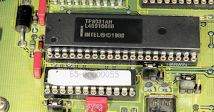
Damaged PAL (IC11)
See the photograph on the right. Notice the dark spot in the middle of the label on the chip next to the 8031 Micro-controller. Initially this looked like a greasy spot, but it turned out to be a 'burn'. The adhesive had been so cooked that the label was effectively bonded to the chip at that point.
Replacing damaged EPROMs is relatively straight-forward, provided you have access to the firmware and a suitable programmer. Recently these have been relatively inexpensive to come by, and the XGecu TL866 is definitely worth the investment. However, the damaged IC on the Remote-Control Decoder turned out to be a PAL ... a different 'animal' altogether.
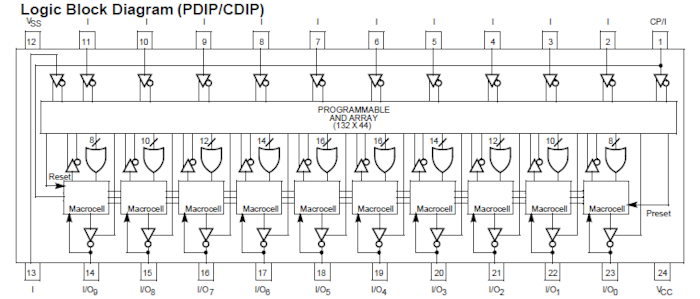
22V10 PAL block diagram
The 22V10 has an impressive 132 x 44 programable AND array and no less than ten programable Macrocells. These devices cannot be readily 'read' since they do not conform to the data structure found in EPROMs etc. But as long as you have the 'map' that was used to configure the array, it is easy to configure a replacement chip using readily available hardware and software. But here's where 'we' ran up against a problem. Despite appealing to the good people at Park Air, as was the case in the past, they informed 'us' that information on the PALs (there are two) in the Remote-Control Decoder could not be provided.
Not only that, we were told that all support for the Series 3000 ceased as far back as 1998 or thereabouts, and that the information that we sought no longer existed. Did that imply that it had been thrown out, or were they (Park Air) simply totally disinterested in providing support? Granted, the type is around thirty years old, but by my reckoning and from what they say, it sounds like they stopped supporting it less than ten years after it went into production! This revelation had both myself and my client completely 'stunned' since both of us had previously worked for major UK Defence Electronics companies that regularly provided very long-term customer support. Not only had Park Air made it clear that support for the type had not been readily available since 1998, they had also declined to provide any information relating to the five mod-strikes, and had also informed my client that such information was never made available to the end-user! Was this actually company policy?
Anyway, back to the current problem ... the faulty PAL. I found that the transceiver would function perfectly as a stand-alone unit without Module-5 fitted. The BITE clearly detected its lack of presence and did not report any issues. However, if Module-5 was installed and IC11 was missing (or faulty), BITE flagged a fault. Whereas a 'locally' operated transceiver is perfectly feasible in a civil ATC context, it is most definitely NOT an option when it is part of a tactical radar installation like the BAe Systems AR-327 (aka T101a). I obtained a couple of 'blank' 22V10s and sent these, along with a working PAL down to my client. As suspected, the security fuse in the working PAL had been blown to prevent readback of the internal programmed pattern. It is probably worth noting here that although AMD CE22V10s have this security fuse, it would appear that Cypress 22V10s might not have this feature.
Being an RF man, logic and such things is not my strong suit. My client informed me that if the PAL was 'protected', they might have to painstakingly etch away the top of the IC in order to wedge-bond a replacement fuse-link in place. But first, his resident expert in such things had a plan whereby patterns would be 'thrown' at a PAL to see if they could mimic the programmed pattern. But that relied on understanding what the PAL was supposed to do, and Park Air had already demonstrated that they weren't interested in helping.
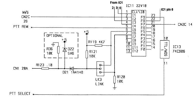
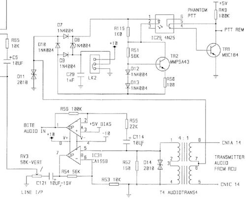
IC11 on Remote Control Decoder
Right: IC11 on the Remote-Control Decoder appears to be primarily associated with rear-panel PTT control, coming onto the board via CN1 pin 20A. From what I can see, there are six (or 7?) inputs and three outputs. Pin 2 is a Mute signal from the Guard Receiver (if fitted). Pin 5 is 'PTT Remote', generated locally (on-board) by TR1. Pin 6 (and perhaps at one time pin 7) handles the Hardwire PTT from the Facilities 2 connector on the rear panel. Pins 1, 3 and 4 are signals from the Microcontroller (IC1)
The three outputs from the PAL are ... Pin 22 which goes to IC1, Pin 21 which goes to the TX Control Module as PTT, and pin 23 provides PTT Select which is an internal control line for enabling Multiplexers IC32 and IC27.
Within the dotted area marked 'Optional' R36 should be R122. As you can see there is already scope for confusion with two different control signals with very similar names ... 'PTT Remote' which is generated on-board and 'Hardwire PTT' which comes from a connector on the rear panel, and thus can be considered Remote PTT. Well done Park Air! And the confusion doesn't end there ...
Para 22 in the Remote-Control Decoder circuit description is, to put it mildly, rubbish. It is entitled Hardwire PTT and reads thus ...
An external hardwire PTT can be configured through the facilities 2 connector and can be set to respond to a ground, or a high (nominally 6V dc) signal (refer to para 10). The signal is connected to the CPU through IC13e and IC11.
Link 2 on Remote Control Decoder
Yes, the signal known as Hardwire PTT does come from the Facilities 2 connector, BUT because of D21 (1N4148), this can be nothing other than a ground connection, i.e. only an Active-Low signal will work. This signal does NOT go to the CPU (mis-named Microcontroller IC1) via IC11 and IC13. Pin 23 of IC11 is an output, NOT and input ... and IC13 is a Hex Open-Drain N-channel Buffer and pin 13 (output) is connected to the Enable pins on multiplexers IC32 and IC27. The only output (presumably PTT-related) from IC11 that goes to IC1, comes from pin 22.
As noted above, Para 22 refers the reader to Para 10. This describes the function of links 2 and 3 on the Remote-Control Decoder. Here, the Active-High signal is given as nominally +24V! Whether it is +6V or +24V, neither will work due to the presence of D21. Note too that Link 2 actually has nothing to do with the Hardwire PTT signal from the facilities connector; rather, it is associated with the 2930Hz PTT-tone via Transformer T4 ... see left.
So ... where's the happy ending?
We have the technology ...
One of my client's engineers, who has a background in chip design, and is apparently very good at it, suggested that it might be possible to ascertain the 'contents' of the PAL (IC11) by 'throwing' patterns at a PAL until it 'mimicked' a known good one. Much easier than slicing away the top and examining the contents under a microscope. After all, the chip only has seven inputs and three outputs. So with the machine on the right, a logic analyser and a 4-channel 'scope, he spent several weeks 'throwing' patterns at a PAL and eventually came up with something that he was 99% sure was a match.
The 'new' PAL, along with an original working one were subsequently sent up to me for testing. It worked! Since IC11's only purpose is to cater for External or Remote PTT, I was very quickly able to verify that the new PAL was working correctly.
Initially I couldn't get either PAL to do anything ... and then it struck me. I had spent the last six months working on these transceivers with them in LOCAL mode. Although the manual clearly states that PTT can be initiated via the 'Facilities 2' connector on the rear panel, what it doesn't say (and I have checked) is that for the connectors on the rear panel to work, the transceiver MUST be set to REMOTE mode.
Not only that. With the manual talking about ac (tone) and dc operation, there was always a question about link settings on the Remote Control Decoder board. Was a simple PTT connection considered as dc? And if tone-PTT (2930Hz tone superimposed on the TX audio) was applied, was that instead of Hardwire-PTT? At the end of the day, with the board configuration un-touched (as received), and the transceiver in REMOTE mode, I found that with 0dbm of 2930Hz applied via the 9-way D-type Remote-1 connector, the transceiver automatically went to Transmit. And with the tone removed, it dropped back to Receive. With no tone present, I found that initiating Hardwire-PTT via the Facilities-2 connector also initiated Transmit.
And there we have our happy ending! Seven faulty Park Air transceivers repaired. I've said it before, and I'll say it again ... I actually like these!
Some light reading ... PAE 3000 manuals:
Operator's Manual
Technical Handbook ... as said, this document contains many errors.