A better 4m PA
5 minute read
Modifying the Tait T199 Power Module for Class AB1
November 2007
Firstly, I have a confession to make. My earlier statement that the power output from my BLY89A-based 4m PA was 35W was grossly optimistic. In hind-sight I can see where the error came from. When measuring the current drawn by the PA, I had omitted to take various other devices into account ... And, well ... The actual output power was only 15W ... NUTS!
Some time ago, I began contemplating a high power 4m PA employing a pair of BLW86’s. Unfortunately, this was a project that was for some reason, blighted with problems. Using John, G3WZT’s excellent guidelines, I came up with a design. John even checked my calculations and was kind enough to point out an error. I was very confident that it would work. But alas, no! I suspect there might actually be a problem with the BLW86 at 70MHz. It is interesting to note from the manufacturer’s data sheet, that the input and output characteristics are given in two parts; above 70MHz and below 70MHz ... Makes you wonder! I blew two devices, or the same device twice, if you know what I mean? I convinced myself that a push-pull amplifier was a non-starter so I knocked up a single stage amplifier having done fresh calculations for the input and output matching networks. I was about to congratulate myself, until I discovered that it was producing almost as much ‘hoot’ as desired power ... NUTS again!
Finally, I turned my attention to the T199 PA blocks which were available from www.technoloya.co.uk at the time. The advantage with these units is that since their heritage is ‘land-mobile’, they operate from 13.8V, unlike the BLW86 which requires 28V. Another distinct advantage is that they are essentially ‘no-tune’ power blocks. Tait have spared no expense in employing high quality Semco mica capacitors throughout.
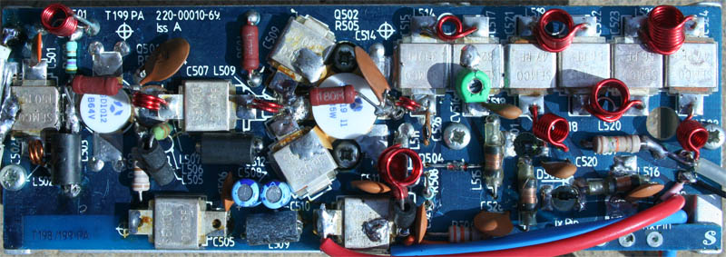
Unfortunately the amplifier is biased for Class-C operation and close examination of the circuit diagram showed that as well as L503 and L510 DC-grounding the bases of each of the two transistors, the driver (SD1012) has a 47R resistor (R502) ‘slugging’ the Base-Emitter junction and the PA device (SD1019/11) has a 22R resistor (R504) in a similar position. It is clearly evident that these two resistors play a critical role in impedance matching and therefore cannot be removed without affecting the overall performance of the amplifier. The solution is to lift the ‘earthy’ ends of each resistor and fit a 1uF chip capacitor between the resistor and ‘ground’. This way the resistor is only effective at RF. This done, the next step is to bias the two transistors for Class-AB1 operation. There are several ways of biasing bipolar transistors but the most effective and reliable circuit is shown below.
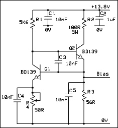
The bias output voltage is the base-emitter junction drop of Q1 plus the drop across R4. R1 must be selected to provide sufficient base drive current for Q2, set by it’s hFE. The only requirement is that Q1’s VBE(f) at that current must be lower than that of the RF transistor at it’s bias current level. The maximum current capability depends on Q2 and R2. The power dissipation of Q2 can be up to a few watts and in most cases should be heat-sinked, but must be electrically isolated from ground. The value of R2 can be calculated as (VCE-VCE (sat))/Ib. Two of these circuits are required (one for each transistor) for the T199 board.
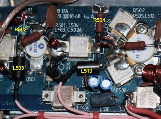
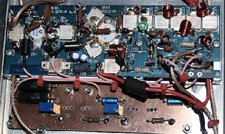
The photograph on the right shows the location of R502, R504, L503 and L504, who’s ‘earthy’ ends require to be desoldered from the ground-plane. The individual bias voltages are then applied to the (now free) ends of L503 (for the SD1012) and L510 (for the SD1019/11).
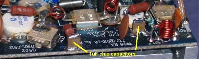
The photograph on the left simply serves to demonstrate the mounting of the 1uF chip capacitors used to DC-isolate resistors R502 and R504 from the ground-plane.
The photograph on the right shows the modified PA module installed along with the bias board described earlier. Note that the BD139 transistors are mounted on the underside of the board. This is to ensure good thermal conduct with the chassis/heatsink. As the PA transistors heat up they require less bias current to maintain the bias point. In turn, VBE for Q1 in each of the bias generators drops as the temperature rises, thus maintaining a stable bias point for each of the two PA transistors.
An added advantage offered by the T199 module is that it comes complete with a PIN-diode T/R switch between the SD1019/11 and the harmonic filter. It made sense to make use of this feature, making it possible to dispense with the large PCB relays previously used. In this configuration, the filter also serves to afford the receiver a modicum of protection from out-of-band interference.
As previously mentioned, this is essentially a no-tune amplifier. There is one tiny trimmer after the PA, but I elected not to touch it. The only adjustment required is the setting of the quiescent current for the two transistors. The easiest way to achieve this is by monitoring the combined collector currents of the two devices. Provided the output from each bias generator is below the base-emitter threshold, the current should be negligible. If it isn’t, something is wrong! I set the quiescent current for the SD1012 at 25-30mA and 45-55mA for the SD1019/1. (Available data regarding the two transistors is sparse, thus the final bias settings may require some tweaking following on-air tests, but these ought to be good starting points). Having previously set the output from the transverter board to 100mW, I applied some RF. With this level of drive, the combined peak PA collector current should be around 5A. It should not be necessary to go beyond 200mW in order to achieve 35W out.
As previously mentioned, this is essentially a no-tune amplifier. There is one tiny trimmer after the PA, but I elected not to touch it. The only adjustment required is the setting of the quiescent current for the two transistors. The easiest way to achieve this is by monitoring the combined collector currents of the two devices. Provided the output from each bias generator is below the base-emitter threshold, the current should be negligible. If it isn’t, something is wrong! I set the quiescent current for the SD1012 at 25-30mA and 45-55mA for the SD1019/1. (Available data regarding the two transistors is sparse, thus the final bias settings may require some tweaking following on-air tests, but these ought to be good starting points). Having previously set the output from the transverter board to 100mW, I applied some RF. With this level of drive, the combined peak PA collector current should be around 5A. It should not be necessary to go beyond 200mW in order to achieve 35W out.